Low-kV scanning electron microscopy (<5 kV) enables highly surface-sensitive imaging with reduced beam damage and minimal sample preparation. Modern desktop SEM systems with STEM detection expand traditional SEM imaging modes and provide an efficient way to screen samples before high-resolution TEM analysis.
Low-kV SEM: Surface-Sensitive Electron Microscopy with Desktop SEM and STEM
Low-kV SEM: Surface-Sensitive Electron Microscopy with Desktop SEM and STEM

SEM vs TEM: When is Transmission Electron Microscopy (TEM) necessary?
Transmission electron microscopy (TEM) is widely used for studying materials and biological structures with atomic- or nanoscale resolution. However, TEM sample preparation is complex and typically involves several steps:
- Fixation
- Dehydration
- Resin embedding
- Ultramicrotomy
- Heavy-metal staining
These processes require specialized laboratory infrastructure, significant preparation time, and experienced operators.
For many research questions—especially during early project stages or rapid sample characterization—such complex preparation may not be necessary. In these situations, low-kV scanning electron microscopy (Low-kV SEM) offers an efficient and practical alternative.
Low-kV SEM: Surface-sensitive imaging at low acceleration voltages
Low-kV SEM typically operates at acceleration voltages below 5 kV. At these lower voltages:
- electron penetration depth is reduced
- the interaction volume becomes smaller
- imaging becomes more surface sensitive
This allows high-contrast visualization of structures close to the sample surface.
Advantages of low-kV SEM
Low-kV scanning electron microscopy offers several important benefits:
- Higher surface sensitivity
- Reduced beam damage for delicate samples
- Lower sample charging
- Reduced need for conductive coatings
- Improved imaging of thin or sensitive materials
These advantages make Low-kV SEM particularly suitable for:
- biological specimens
- polymers and soft materials
- nanostructured surfaces
- beam-sensitive samples
- thin films and layered materials
In life sciences, nanotechnology, and materials research, Low-kV SEM often provides sufficient structural information without requiring complex TEM preparation.
STEM in SEM: Additional contrast mechanisms
Modern scanning electron microscopes can also include STEM detection (Scanning Transmission Electron Microscopy). This allows the detection of electrons transmitted through thin samples, expanding the imaging capabilities of SEM.
An example is the Thermo Scientific Phenom Pharos FEG Desktop SEM, a high-performance field-emission SEM optimized for high-resolution imaging at low acceleration voltages.
By using a STEM holder for desktop SEM, transmitted electrons can be detected in addition to conventional SEM signals.

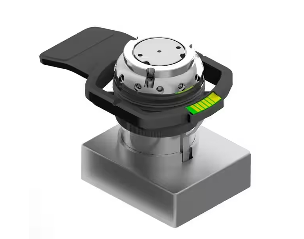
SEM and STEM imaging modes
Traditional SEM imaging modes include:
- Secondary Electron (SE) imaging
- Backscattered Electron (BSE) imaging
With STEM detection, additional contrast mechanisms become available:
- Bright-Field STEM (BF)
- Dark-Field STEM (DF)
- HAADF-STEM (High-Angle Annular Dark Field)
These signals provide mass-thickness and scattering-angle dependent contrast, allowing researchers to obtain additional information about:
- material density
- nanostructures
- morphology
- compositional variations
Desktop SEM as a sample screening tool for TEM
The combination of Low-kV SEM and STEM detection is particularly useful as a pre-screening step in electron microscopy workflows.
In this approach, samples are first examined with SEM to identify promising regions. Only those regions are subsequently analyzed using high-resolution TEM.
This workflow offers several advantages:
- reduced sample consumption
- shorter preparation times
- more efficient use of TEM instrument time
- avoidance of unnecessary TEM measurements
In many applications, fine structural details can already be detected using Low-kV SEM, meaning TEM is only required for targeted high-resolution analysis.


Application example: Cryo-EM sample screening
This approach is becoming increasingly important in cryo-electron microscopy (Cryo-EM) workflows.
Desktop STEM systems can be used to quickly identify suitable sample areas on TEM grids before performing time-consuming Cryo-EM measurements.
This improves overall efficiency and reduces unnecessary Cryo-EM instrument time.
Conclusion
Low-kV scanning electron microscopy provides a powerful method for surface-sensitive analysis of materials and biological samples. When combined with STEM detection in modern desktop SEM systems, it enables efficient sample characterization with minimal preparation effort.
As a pre-screening tool before TEM or Cryo-EM analysis, Low-kV SEM can significantly accelerate microscopy workflows while reducing costs and resource consumption.
Frequently Asked Questions (FAQ)
What is Low-kV SEM?
Low-kV SEM refers to scanning electron microscopy performed at low acceleration voltages (typically below 5 kV). This reduces beam penetration depth and enables highly surface-sensitive imaging.
What is the difference between SEM and TEM?
SEM primarily images sample surfaces, while TEM transmits electrons through thin samples to reveal internal structures at extremely high resolution.
What is STEM detection in SEM?
STEM in SEM detects electrons transmitted through thin samples, providing additional contrast modes such as bright-field, dark-field, and HAADF imaging.
Why use Low-kV SEM before TEM?
Low-kV SEM enables rapid sample screening to identify relevant regions before performing time-consuming TEM measurements.

Looking for the right solution?
Get in touch with our experts.


